

PLD Terms
A chip that contain relatively large amounts of logic circuitry with a structure that is not fixed, called Programmable Logic Device (PLD). In general, a programmable logic device is a circuit, which can be configured by the user to perform a logic function. Unlike a logic gate, which has a fixed function, a PLD has an undefined function at the time of manufacture. Before the PLD can be used in a circuit, it must be programmed (reconfigured). PLD provides specific function, such as electronic decoder, driver, counter and other function a system must perform.
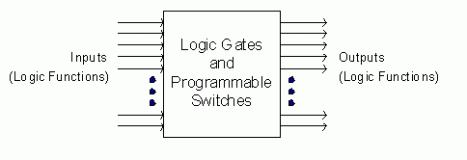
Figure 1. PLD Block Diagram
Programmable logic device (PLD) can be changed at any time to perform any number of functions. The designers may use inexpensive software to develop, simulate and test their design. After that, the designers can test PLD in a real circuit. They also can change the circuit easily to their satisfaction. This can be done because PLD is based on rewriteable memory technology.
In middle 1978, the inventors of Monolithic Memories, Inc (MMI), John Birkner and H.T. Chua introduced Programmable Array Logic (PAL). This device equipped with PROM (Programmable read-Only Memory) and additional logic gates.The software design tool is PALASM (PAL Assembler).This software makes PAL easy to use. MMI made agreements with AMD, National, and TI to established the 20-pin bipolar devices (PAL16L8, PAL16R8, etc).
Another innovation of PAL invented by Lattice Semiconductor is Generic Array Logic (GAL). The GAL is erasable and re-programmable. It is also able to take place of many PAL devices and also wider PAL original function. These advantages makes easier for designers to prototype and change their design.
In general, there are three different type of PLD: Simple Programmable Logic Device (SPLD), Complex Programmable Logic Device (CPLD), and Field Programmable Logic Device (FPGA). The SPLD device typically contains about 600 or fewer gates, meanwhile the CPLD contains up to 10,000 gates. The FPGA contains the highest amount of gates and highest performance. The FPGA may contains hundred of thousands gates. Therefore, CPLD and FPGA are often referred as High Capacity Programmable Logic Device (HCPLD).CPLD is often used in portable applications such as mobile phone, personal digital assistant, etc. Meanwhile FPGA is used widely in data processing and storage, instrumentation system, telecommunications, and digital signal processing.
Complex Programmable Logic Device (CPLD) is a high-density programmable device generally based on the PAL or SPLD architecture. Its routing is more predictable timing than FPGA.
Field Programmable Gate Array (FPGA) is a single chip contains gate array, with general-purpose metal tracks, often with variable length segments or routing tracks. The device is programmed by turning on the switches, which makes connections between circuit nodes and the metal routing tracks. The term Programmable Logic means that a logic element whose function is not restricted to a specific function. The designer can program it using a programming software tool. The term Gate Array means the gates are fabricated in a 2 dimensional array on a die to form a specific function such as phase lock loops, delay-locked loops, SRAM blocks and others.
The connection between circuit nodes and the metal routing tracks may be made by a transistor switch (which is controlled by a programmable memory element) or by an antifuse. An antifuse is an electrical device that performs the opposite function to a fuse. Whereas a fuse starts with a low resistance and is designed to permanently break an electrically conductive path (typically when the current through the path exceeds a specified limit), an antifuse starts with a high resistance and is designed to permanently create an electrically conductive. (http://en.wikipedia.org/wiki/Antifuse)
Filed under: Technology | Tagged: asia, bali, balinese, balinese archive, CPLD, denpasar, FPGA, GAL, indonesia, PAL, PAL16L8, PAL16R8, pekambingan, PLD, PNB, sapteka, SPLD, Technology | 1 Comment »


